Optically and magnetically active point
defect centers in semiconductors may realize as quantum bit candidates for quantum computing. One of the exemplary and most studied centers is the
nitrogen vacancy (NV) center in diamond. This system exhibits triplet electronic spin that can be coherently manipulated and can be read out as a qubit even at room temperature by optical means. Over the years, a plethora of non-characterized defect centers were created in various semiconductor materials. Therefore, among those there might be ones that possess even better properties than that of NV for quantum technologies. However, the
many properties of these defect centers, optical centers, electron paramagnetic resonance (EPR) centers are left unknown in experimental measurements.
Additionally, there are various technological challenges to overcome for defect-based qubits and quantum emitters that still limit the defect qubit applications “en masse”. Mainly, these challenges are related to the loss of coherence within qubits which is especially important when the qubits are entangled together as a solid-state spin qubit register. For example, magnetic dipole-dipole interaction between the qubit and neighboring spins of other defects or nuclei can be the source of such relaxation. Additional unavoidable decoherence channels may appear due to thermal
phonons of the host material known as "spin-lattice"
Orbach relaxation. Interactions with phonons are not limited to spin-phonon terms as the much stronger electron-phonon interaction (
for example within the Huang-Rhys approximation) may impose severe limitations on the
applicability of defects. The PhD student would emerge in such theories and unravel the
applicability of ab-initio calculations on
first and second order (Raman) phonon interactions which terms govern the coherence properties of defect qubits.
Recently, the focus of quantum applications with defects shifted to charge state stability. In simple words, various color centers in diamond or silicon-carbide
undergo the phenomenon called "
bliking" - eg. their luminescent signal is
continuously turned on and off under strong laser excitation severely limiting real-world applicability. The blinking phenomenon is mostly believed happen due to charge state change upon saturated illumination. Therefore, the PhD applicant will be tasked for calculate such phenomena:
radiative and non-radiative pathways,
photoionization cross-sections, group theoretical considerations (
selection rules) to give an experimentally realible holistic overview picture about how exactly the blinking occurs and which excited states are being involved and activated.
Therefore, the PhD student would
unravel the physical nature of these defect centers embedded in diamond and other semiconductors (silicon, silicon-carbide, 2 dimensional boron-nitride, etc.) by means of density functional theory (DFT)
calculations on the electronic structure within and beyond the Born-Oppenheimer approximation. Additionally, other interactions may also govern the physical processes of defect centers:
spin-orbit coupling, hyperfine coupling,
magnetic spin-spin interaction,
nuclear quadrupole interaction,
electron-phonon and spin-phonon coupling, various forms of electron-phonon coupling such as
Jahn-Teller instability or
Huang-Rhys theory – all of them may be a key element for actual real-world qubit realizations utilizing defects. Yet, not all of these physical properties can be measured directly by experimental methods thus suggesting the need of
theoretical simulations from first principles to unravel such "hidden" properties.
These hidden properties are often unknown during experimental measurements and, thus often empirical recipes are used at the moment to avoid the aforementioned mentioned "blinking". Current quantum computing, quantum sensing, quantum communication applications utilizing color centers (defects in solids) are already reached
industrial implementation stage by various companies, startups (
Quantum Brilliance,
Diatope,
Qdti,
Nvision,
Element six), yet the scalability of their implementations are often limited by charge state control - loss of the signal - thus the blinking. Therefore, the results may contribute for realization of qubits in solids or greatly improve the already known defect centers by optimization. Additionally, the PhD student may develop and improve the ab-initio codes and apply them on the selected defect centers of the Research Topic that may approximate the relaxation and coherence times directly from first principles. These studies will be carried out in close collaboration with domestic and international partners (Ulm University or Max Planck Institute for Polymer Research at Mainz, Germany for example). The ab-initio calculations will be run on the
computer cluster. The
research group that research group is simultaneously split between
BME “FA” building and
Wigner RCP.
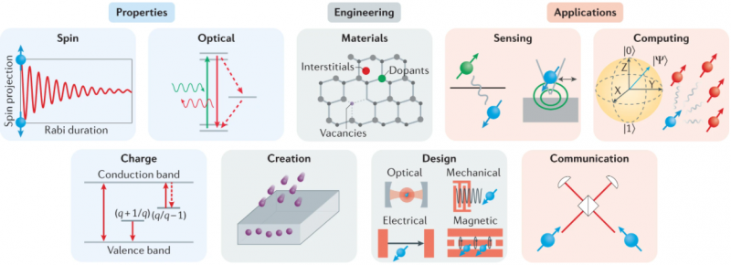 Illustration of key concepts in the field, highlighting the three major defect properties (spin, optical and charge) in the blue panels, engineering considerations (materials, creation and design) in the grey panels and the three major quantum applications (sensing, communication and computing) in the red panels. Ref. Wolfowicz, G., Heremans, F.J., Anderson, C.P. et al. Quantum guidelines for solid-state spin defects. Nat Rev Mater 6, 906–925 (2021). https://doi.org/10.1038/s41578-021-00306-y